EN
EN AR
AR FR
FR DE
DE HI
HI IT
IT JA
JA KO
KO PT
PT RU
RU ES
ES ID
ID LV
LV VI
VI HU
HU MS
MS GA
GA BE
BE YI
YI EU
EU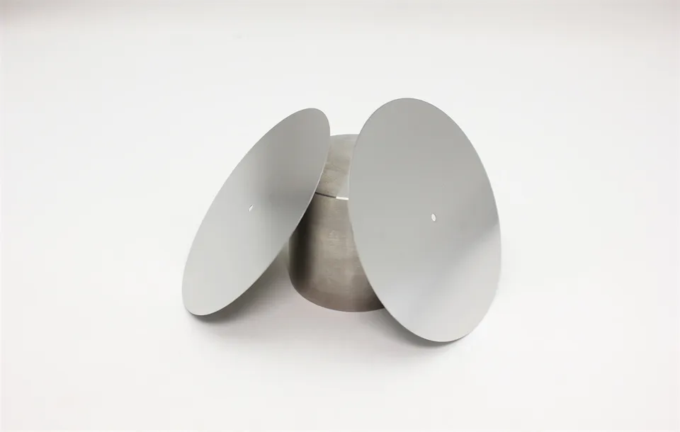
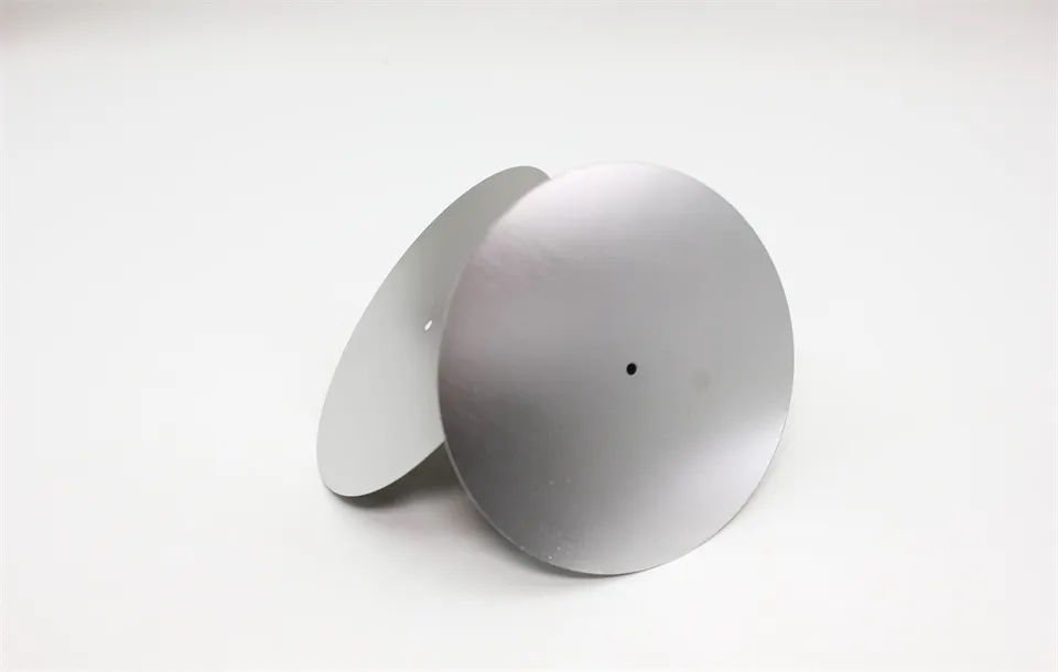
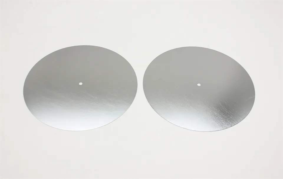
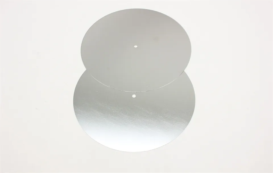
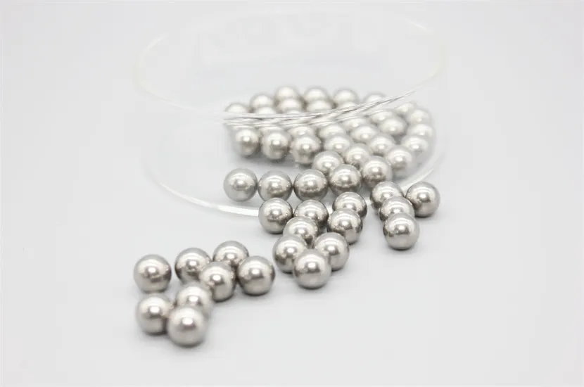
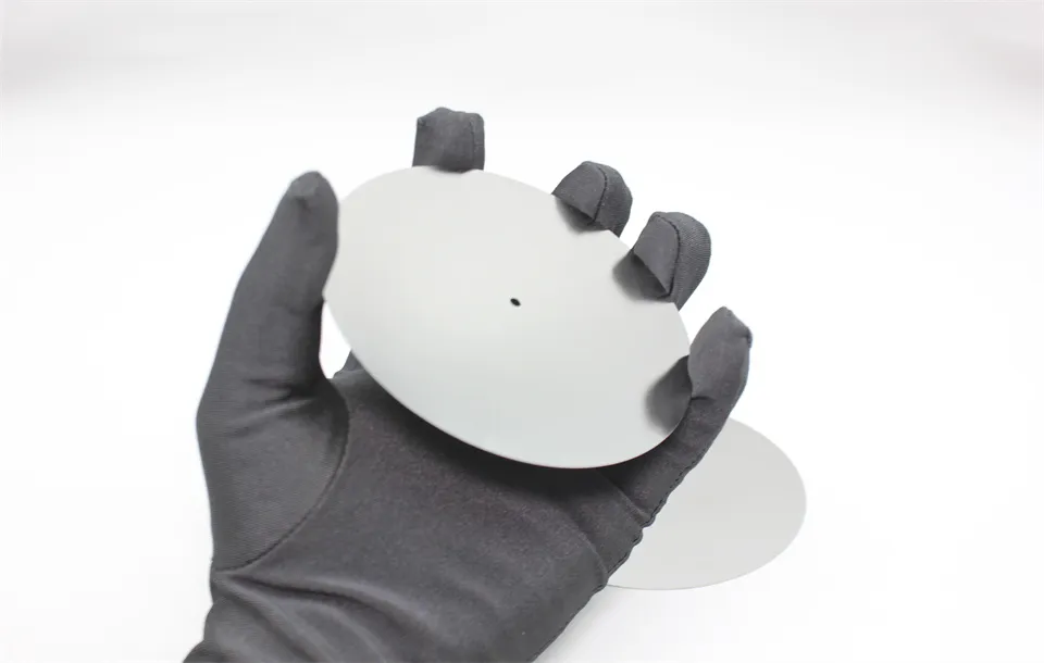
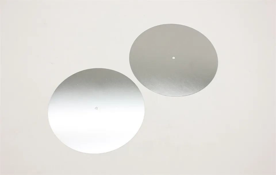
High Purity Polished Tungsten Wafer
| Payment Type: | T/T |
| Incoterm: | FOB,CIF,EXW,FCA,Express Delivery |
| Min. Order: | 2 Kilogram |
| Transportation: | Ocean,Air,Express |
Attributes
Model No.: JDTG-TW-001
Brand: ZZJD
Place Of Origin: China
Size: Support customization Length&Diameter
Material: Tungsten
PACKAGING & DELIVERY
Package Type : Standard export packing
DESCRIPTION
Tungsten alloy wafers are specialized materials used in various high-tech applications, particularly in the semiconductor and electronics industries. Here are some key points about tungsten alloy wafers:
1. Composition: Tungsten alloys typically consist of tungsten combined with other metals like nickel, iron, or copper.
2. Properties:
- High melting point (up to 3422°C)
- Excellent thermal conductivity
- Good electrical conductivity
- High density and strength
- Resistance to corrosion and wear
3. Applications of Tungsten wafer:
- Semiconductor manufacturing equipment
- X-ray targets
- Radiation shielding
- High-temperature furnace components
- Military and aerospace parts
4. Manufacturing process:
- Powder metallurgy techniques
- Sintering at high temperatures
- Precision grinding and polishing to achieve desired thickness and flatness
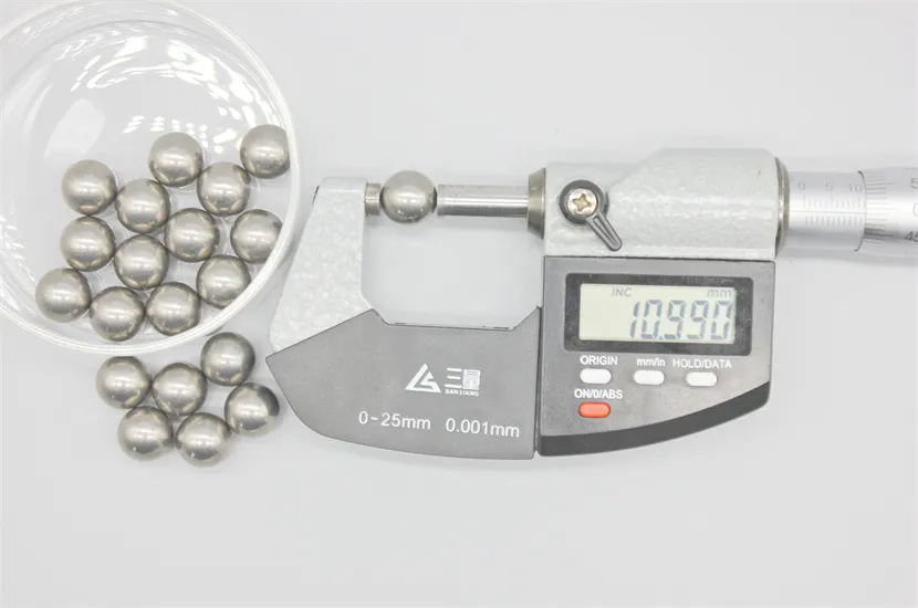
5. Specifications:
- Typically available in thicknesses ranging from 0.1 mm to several millimeters
- Diameter can vary, but common sizes include 100mm, 150mm, and 200mm
6. Surface finish:
- Can be polished to very smooth finishes (e.g., <10 nm Ra)
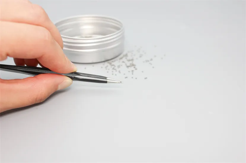
7. Customization:
- Can be produced in various shapes and sizes based on specific application requirements
8. Quality control:
- Strict dimensional tolerances and material consistency are maintained
9. Cost:
- Generally more expensive than standard metal wafers due to the specialized nature of tungsten alloys
10. Research and development:
- Ongoing work to improve properties and develop new applications for these materials